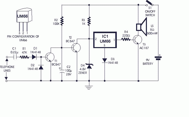
Telephone In-Use Indicator


Circuit : Miroslav Adzic

Description:
This circuit will illuminate a LED if one of your telephones is in use. It should work in all countries (Including UK) that have a standing line voltage above 48 Volts DC.

Webmasters Note:
Please note that it is illegal to make a physical permanent connection to your telephone line in some countries (this includes the UK and Ireland). If building this circuit it is advisable to use a plugin cord so that the unit can be unplugged should a fault occur. If in doubt consult either your telephone or cable operator.

in use indicator

Notes:
If all extension phones are on-hook and the line voltage is around 48 V, Q1 will conduct thus effectively shorting the gate of Q2 to its source, so it will be off and the LED will be disabled.

Lifting the handset of any phone on the line causes the line voltage to drop to 5-15 V. The gate voltage of Q1, equal to some 6% of the line voltage, will then be too low and Q1 will be turned off. So Q2's gate is now biased at approximately 1/2 of the line voltage, Q2 turns on and the LED indicates that the line is in use. The circuit itself is practically invisible to the other telephone devices using the same line.

LED1 must be low-current and its current-limiting resistor must be 2k2 or more. The other components' ideal values may vary slightly, depending on the local telephone line parameters. The circuit is powered off the telephone line.

If other types of MOSFETs are used, the 500k trimmer can be adjusted to ensure that Q1 is biased fully on while the line is not in use (LED1 off), and vice versa. If Q2 is not a BS108 but some other 200 V MOSFET with a higher G-S threshold voltage, it might be necessary to increase the value of the lower (or decrease the value of the upper) one of the two resistors connected to the gate of Q2.

Plain (bipolar junction) transistors can be used instead and the circuit also works fine, but the resistor values are then much lower - letting ten times more microamps of current pass through while the line is not in use, and even this MOSFET design still could not meet formal minimum on-hook DC resistance specifications.

Both prototypes' PCBs were 4x1 cm. The current-limiting resistor for LED1 is 2k2 in both cases. DO NOT ground any of the leads or conducting surfaces in this circuit. A more reliable design would also include some kind of over-voltage protection etc.

Warning:
In their normal course of operation, telephone lines can deliver life-threatening voltages! Do not attempt to build any of the circuits/projects unless you have the expertise, skill and concentration that will help you avoid an injury.

There are also legal aspects and consequences of connecting things to telephone lines, which vary from country to country. Keep away from telephone lines during a lightning storm!

Source: http://www.zen22142.zen.co.uk

Phone In Use Indicator With this circuit mounted in or near every phone in the house, it will allow users to know if the phone is being used and not


Phone In Use Indicator

With this circuit mounted in or near every phone in the house, it will allow users to know if the phone is being used and not to pick up the phone. When a phone is taken off hook, the voltage across the tip and ring terminals drops to 10 volts or less. This will cause the FET (2N4360) to turn on and also turn on the transistor (2N2222). When the transistor turns on it will allow current to flow through the LED and make it light. A blinking LED could be used to make the effect better

.

Phone In Use Indicator

Source: http://www.home.maine.rr.com

Telephone line monitor Telephone line monitor If you feel that somebody is tampering with your telephone line you might find this little circuit


Telephone line monitor

Telephone line monitor

If you feel that somebody is tampering with your telephone line you might find this little circuit useful. It detects if there is another telephone connected to the line, if there is a short or an open line. Sound and a flashing light will tell you which is the current situation. The speaker is practically cut out during a normal conversation thus preserving privacy, only the LED will flash occasionally. The circuit does not require any battery and takes the supply from the telephone line itself. The transistors used are wired in a reversed biased fashion thus behaving as oscillators. You might try the 2N2222A as an alternative (not tested). This monitor is, of course, suitable only for analogue lines. Watch the polarity of the input line: the circuit will not be damaged by a polarity reversal but it will not operate correctly.

Cut Phone Line Detector A while ago I got an email asking for the schematic of a circuit to detect cut phone


Cut Phone Line Detector

A while ago I got an email asking for the schematic of a circuit to detect cut phone lines. It didn't take me long to find this circuit in Electronics Now. When the circuit detects that a phone line has been cut, it activates a MOSFET which can be used to drive a relay, motor, etc. It can also be connected to a security system.

Schematic


This is the schematic of the cut phone line detector

Parts


Part

Total Qty.

Description

Substitutions

R1, R2, R3

3

22 Meg 1/4 W Resistor


R4

1

2.2 Meg 1/4 W Resistor


C1

1

0.47uF 250V Mylar Capicitor


Q1

1

2N3904 Transistor

2N2222

Q2

1

2N3906 Transistor


Q3

1

IRF510 Power MOSFET


D1

1

1N914 Diode


Load

1

See "Notes"


MISC

1

Wire, Phone Connectors, Circiut Board


Notes

1. The "Load" can be a relay, lamp, motor, etc. The circuit can also be connected to a security system to sound an alarm in case the phone line is cut.

2. If the circuit is connected to a security system or other circuit, both circuits must be electrically isolated from each other using an opto-isolator, relay, etc. This also means that the Cut Phone Line Detector must be powered by a seperate 9V supply.

Telephone amplifier While talking to a distant subscriber on telephone, quite often we feel frustrated when the voice of the distant subscrib


Telephone amplifier

While talking to a distant subscriber on telephone, quite often we feel frustrated when the voice of the distant subscriber is so faint that it is barely intelligible. To overcome the problem, circuit of an inexpensive amplifier is presented here. It can be assembled and tested easily. There is no extra power source needed to power up the circuit, as it draws power from the telephone line itself. The amplifier will provide fairly good volume for the telephone conversation to be properly heard in a living room. A volume control is included to adjust the volume as desired.
The circuit is built around IC LM386. Diodes D6 and D7 are used to limit the input signal strength. Transformer X1 is a transistor radio's output transformer used in reverse. As original secondary (output) winding is connected in series with the telephone lines, the speech signals passing through the lines cause change in the magnetic flux in the core of transformer and thereby induce signal voltage across the primary winding. This audio signal is used as input for IC LM386. Diodes D2 through D5 connected in bridge configuration constitute a polarity guard so that the amplifier is powered with correct polarity, irrespective of the line polarity, Zener diode D1 may have any breakdown voltage between 6 and 12 volts range. e.


There is no need of a separate power switch as the circuit energises (via the normally open contacts of the cradle switch) when one lifts the handset.
The circuit may be wired on a general-purpose PCB or by etching a PCB for this circuit.
The circuit can be easily tested by connecting a 6 volts supply to line terminals 1 and 2. A hissing sound will be heard from the loudspeaker. Now connect 6V AC from a transformer to terminals 1 and 2 and observe hum in the loudspeaker. The volume of the hum can be changed through potentiometer VR1. Diodes D6 and D7 limit the input below ± 700 mV.
The circuit is to be connected to the telephone lines in series with the telephone instrument, as shown in the figure

Telephone amplifier

Click on the image to view the full

Soft Musical Telephone Ringer The normal telephone bell, at times (specially during night when one does not want to be disturbed), appears to be


Soft Musical Telephone Ringer

The normal telephone bell, at times (specially during night when one does not want to be disturbed), appears to be quite irritating. The circuit shown here converts the loud sounding bell into a soft and pleasing musical tone.


The incoming ring is detected by transistor T1 and components wired around it. In absence of ringing voltage, transistor T1 is cut off while transistor T2 is forward biased as resistor R2 is returned to the positive supply rails. As a result collector of transistor T2 is at near-ground potential and hence IC1 (UM66) is off. Also capacitor C2 is charged to a slightly positive potential.


During positive half of the ringing voltage, diode D1 forward biases transistor T1 and rapidly discharges capacitor C2 to near ground potential and cuts off transistor T2 which, in turn, causes IC1 to be forward biased and music signal is applied to base of transistor T3 which drives the speaker. During negative half of the ringing voltage, capacitor C2 cannot charge rapidly via resistor R2 and hence transistor T2 remains cut off during the ringing interval. Thus the soft musical note into the loudspeaker sounds in synchronism with the ringing signal. When handset is lifted off the cradle, the ringing voltage is no more available and hence the soft musical note switches off.

Soft Musical Telephone Ringer

Click on the image to view the full

Phone "Hold" With Music Phone Hold With Music This circuit will allow you to place a phone call on hold and if you wish to have them listen to mu


Phone "Hold" With Music

Phone Hold With Music

This circuit will allow you to place a phone call on hold and if you wish to have them listen to music while they are on hold. The circuit operates as follows: The RED wire from the phone jack is typically positive and the GREEN wire is negative or ground. When you want to place a call on hold, close S1 and hang up the handset. The resistor R1 simulates another phone off hook and allows enough

current to pass through to prevent the phone company from disconnecting the call. The resistor R2 and LED provide a visual indication that you have someone on hold ( this is optional )

The capacitor C1 and the transformer provide the interface to a radio or CD player headphone jack. Before you hook up the project to the phone line you must determine the polarity of the line. Place a voltmeter across the red and green wires of the telephone line, there should be about 48 volts

DC positive when the black lead of your meter is connected to the green phone wire. If it is negative 48 volts then reverse the wires.

Phone line indicator With this circuit you can monitor your telephone line. You are able to detect if any telephone in the same line is busy w


Phone line indicator

With this circuit you can monitor your telephone line. You are able to detect if any telephone in the same line is busy with the help of a LED. This circuit does not affect the telephone's line provider, so it's trouble free but you use it at your own risk.

It connects in parallel with the telephone line. The bridge rectifier (D1...D4) at the input protects the circuit from reverse polarity. When none of the telephones of this line is used then the voltage across the line is about 50-60V. This voltage with the help of the bridge and R1/R2 voltage divider affects the gate of BF256B so it stays in non conductive mode. When a telephone is used the voltage across the line drops suddenly and Ô1 goes to conductive mode so the Led lights up, giving us the "in use indication".

Phone line indicator

In Ô1 the current which flows through LED is about 10mÁ. The zener diode D5 prevents gate's voltage to excess 10V and C1 works like a filter for unwanted pulses. If your circuit doesn't work ok , you can replace R1 with another, but no more that a 220ÊÙ one.

The circuit works ok with a 9V battery and you can put it into a plastic box.
Attention:
50V from the telephone line can become dangerous under some circumstances so take precautions when handling it.

PCB

telephone2-2.gif telephone2-3.gif

Parts List

R1= 100K
R2= 1M
C1=1ì/63V
T1=BF256B
D1..D4=1N4004
D5= 10V/1W
D6=Led red

Cellular Phone calling Detector Flashes a LED when detecting an incoming call Powered by one 1.5V cell


Cellular Phone calling Detector


Flashes a LED when detecting an incoming call

Powered by one 1.5V cell

Cellular Phone calling Detector


Parts:

R1____________100K   1/4W Resistor R2______________3K9  1/4W Resistor R3______________1M   1/4W Resistor  C1,C2_________100nF   63V Polyester Capacitors C3____________220µF   25V Electrolytic Capacitor  D1______________LED  Red 10mm. Ultra-bright (see Notes) D2___________1N5819  40V 1A Schottky-barrier Diode (see Notes)  Q1____________BC547   45V 100mA NPN Transistor  IC1____________7555 or TS555CN CMos Timer IC  L1_____________Sensor coil (see Notes)  B1_____________1.5V Battery (AA or AAA cell etc.) 

Device purpose:

This circuit was designed to detect when a call is incoming in a cellular phone (even when the calling tone of the device is switched-off) by means of a flashing LED.
The device must be placed a few centimeters from the cellular phone, so its sensor coil L1 can detect the field emitted by the phone receiver during an incoming call.

Circuit operation:

The signal detected by the sensor coil is amplified by transistor Q1 and drives the monostable input pin of IC1. The IC's output voltage is doubled by C2 & D2 in order to drive the high-efficiency ultra-bright LED at a suitable peak-voltage.

Notes:

  • Stand-by current drawing is less than 200µA, therefore a power on/off switch is unnecessary.

  • Sensitivity of this circuit depends on the sensor coil type.

  • L1 can be made by winding 130 to 150 turns of 0.2 mm. enameled wire on a 5 cm. diameter former (e.g. a can). Remove the coil from the former and wind it with insulating tape, thus obtaining a stand-alone coil.

  • A commercial 10mH miniature inductor, usually sold in the form of a tiny rectangular plastic box, can be used satisfactorily but with lower sensitivity.

  • IC1 must be a CMos type: only these devices can safely operate at 1.5V supply or less.

  • Any Schottky-barrier type diode can be used in place of the 1N5819: the BAT46 type is a very good choice.

  • Source: RED Free Circuit Designs

Alcatel 311/511 (BF, BF3, BF4) cell phones for data/flash cable only 5 pin Alcatel 311 cellphone special 5 pin Alcatel 311 cellphone special connector


Alcatel 311/511 (BF, BF3, BF4) cell phones

for data/flash cable only

 5 pin Alcatel 311 cellphone special
5 pin Alcatel 311 cellphone special connector at the mobile phone (keypad up)
Mobile phone interface pinDescription
1Gnd
2AT RCK
3TA ARQ
4TA MS TX
5TA MS RX
Data/flash cable

Source:www.pinouts.ru

Take me back to a simpler time, Radio Flyer Google Electronics Infoline Web Follow us on Twitter Take our 5 minutes Survey and win $100 Visa Gi


Take me back to a simpler time, Radio Flyer


Take me back to a simpler time, Radio Flyer

[Fred Keller] and [Judy Foster], both retired, are proving that age is just a number. What you see above is a nostalgia inducing full size driveable Radio Flyer red wagon. The base of which is a 1976 Mazda pickup truck, while the wagon portion is a mishmash of wood, fiberglass and bondo, detergent bottles, and more. Even the steering wheel has been retrofitted from an actual wheel from a wagon. We were surprised to find out the entire conversion only took the two 11 months to complete (finishing this past august), and even more confounded to learn the vehicle is completely street legal.

[Thanks Rob]

0diggsdigg
Via Hack a Day, Published: 2010.10.18

Intelligent Robot-Like Spider Known as Eigenbau


Intelligent Robot-Like Spider Known as Eigenbau

The project aims to develop the Eigenbau robot spider that is well-programmed with Javelin Stamp microcontroller.

Mobile phone radiation and health concerns have been raised


Mobile phone radiation and health concerns have been raised, especially following the enormous increase in the use of wireless mobile telephony throughout the world. This is because mobile phones use Electromagnetic radiation in the Microwave range. These concerns have induced a large body of research in animals and in humans

The mobile phone system is referred More >

Post from: Electronic circuits and projects

Motion Sensor Switch for alarm, light or water sprinkler


The Motion Sensor Switch circuit is a motion sensor controlled automatic water sprinkler but you can easily add an alarm/light function too. Before beginning the construction contact your nearest electronics component vendor and procure a readymade box-type Passive Infrared (PIR) Motion Sensor unit. Such units, packed in a compact enclosure with power input and relay output terminals are widely available.


In prototype, an unbranded (Made in China) PIR Motion sensor with the following specifications are used.
  • Detection Range:10Meter Maximum
  • Supply Input:12V DC, <500ma
  • Relay Output :Common(C),Normally Closed(N/C),Normally Opened(N/O)
  • Relay ON time: 15 Secs (Not Adjustable)

pir motion sensor unit

Now install the PIR module hanging from a 3 metre high mast (to cover 10 metre radius area) and connect its supply and relay terminals to our finished and enclosed circuit, observing right polarity. A 4-core screened cable can be used for this interconnection. Power the circuit from a regulated 12VDC adaptor/solar power box.

Whenever the PIR module detect movement of a live body its relay output toggles and the switching mosfet (T1) in the circuit is switched to on via resistor R1 and related parts. As as result, the EM relay at the output of T1 is activated and the electric sprinkler gets its supply through the relay (RLY1) contacts. This contacts (or spare contacts) can also be used to activate a high-power warning alarm.

Please note that, here T1 is wired as a mini electronic timer. Even after the PIR relay switched off, output relay (RLY1) remains in on state for a short duration decided by the value of timing capacitor C2.

Motion Sensor Switch Circuit Schematic

motion sensor switch circuit schematic

The Electric Sprinkler

electric sprinkler


Solar Lights for Outdoor Garden project


This Outdoor LED Solar Garden Lights project is a hobby circuit of an automatic garden light using a LDR and 6V/5W solar panel. During day time, the internal rechargeable 6 Volt SLA battery receives charging current from the connected solar panel through polariy protection diode D9 and current limiting resistor R10. If ambient light is normal, transistor T1 is reverse biased by IC1 (LM555).
Here IC1 is wired as a medium current inverting line driver, switched by an encapsulated light detector (10mm LDR). Multi-turn trimpot P1 sets the detection sensitivity. When ambient light dims,transistor T1 turns on to drive the white LED string (D1-D8). Now this lamp load at the output of T1 energises. Resistors R1-R8 limits the operating current of the LEDs. When the ambient light level restores, circuit returns to its idle state and light(s) switched off by the circuit.

Assemble the Outdoor Solar Lights circuit on a general purpose PCB and enclose the whole assembly in a transparent plastic box. Drill suitable holes on the top of the encloure to mount the mini solar panel (SP1) and the light sensor (LDR), and in front for fitting power switch (S1) and the sensitivity controller (P1).

Fix the battery inside the cabinet using a double-sided glue tape/pad. Finally, the LDR should not be mounted to receive direct sunlight. It must be mounted at the top of the enclosure, pointing to the sky say southwards. This circuit is very simple. So interested and experienced hobbyists can alter/modify the whole circuit as per their own ideas without any difficulty (Just try a 6V relay with T1 to drive more number of LED strings)

Outdoor LED Solar Lights Circuit Schematic

outdoor garden solar lights circuit schematic

Smart Heater Controller Latest Project


Minuscule circuit of the electronic heater controller presented here is built around the renowned 3-Pin Integrated Temperature Sensor LM35 (IC1) from NSC. Besides, a popular BiMos Op-amp CA3140 (IC2) is used to sense the status of the temperature sensor IC1, which also controls a solid-state switch formed by a high power Triac BT136(T1). Resistive type electric heater at the output of T1 turns to ON and to OFF states as instructed by the control circuit. This gadget can be used as an efficient and safe heater in living rooms, incubators, heavy electric/electronic instrument etc.
Normally, when the temperature is below a set value (Decided by multi-turn preset pot P1), voltage at the inverting input (pin2) of IC1 is lower than the level at the non-inverting terminal (pin3). So, the comparator output (at pin 6) of IC1 goes high and T1 is triggered to supply mains power to the desired heater element.

When the temperature increases above the set value, say 50-60 degree centigrade, the inverting pin of IC1 also goes above the non-inverting pin and hence the comparator output falls. This stops triggering of T1 preventing the mains supply from reaching the heater element. Forunately, the threshold value is user-controllable and can be set anywhere between 0 to 100 Degree centigrade.

The circuit works off stable 9Volt dc supply, which may be derived from the mains supply using a standard ac mains adaptor (100mA at 9V) or using a traditional capacitive voltage divider assembly. You can find such power circuits elsewhere in this website.

Note:CA3140 (IC2) is highly sensitive to electrostatic discharge (ESD). Please follow proper IC Handling Procedures.

Electronic Heater Controller Circuit Schematic

electronic heater controller circuit schematic

Latest Digital Thermometer DIY project


This diy digital thermometer circuit can measure temperatures up to 150°C with an accuracy of ±1°C. The temperature is read on a 1V full scale-deflection (FSD) moving-coil voltmeter or digital voltmeter.
How the digital thermometer works

Operational amplifier IC 741 (IC3) provides a constant flow of current through the base-emitter junction of npn transistor BC108 (T1). The voltage across the base-emitter junction of the transistor is proportional to its temperature. The transistor used this way makes a low-cost sensor. You can use silicon diode instead of transistor.

The small variation in voltage across the base-emitter junction is amplified by second operational amplifier (IC4), before the temperature is displayed on the meter. Preset VR1 is used to set the zero-reading on the meter and preset VR2 is used to set the range of temperature measurement.

Operational amplifiers IC3 and IC4 operate off regulated ±5V power supply, which is derived from 3-terminal positive voltage regulator IC 7805 (IC1) and negative low-dropout regulator IC 7660 (IC2). The entire circuit works off a 9V battery.

Assemble the circuit on a general-purpose PCB and enclose in a small plastic box. Calibrate the thermometer using presets VR1 and VR2. After calibration, keep the box in the vicinity of the object whose temperature is
to be measured.

Sent by Mihail Dorutz, CH. Thanks a lot!

Digital Thermometer Circuit Schematic

diy digital thermometer circuit schematic

PWM RGB Controller


The design of a Pulse Width Modulated Red-Green-Blue controller will be explained here. This design is efficient because this design uses multiple strings of six LEDs with a 24V DC source. This design is sufficient for a sizeable light because a total current of 2 Amps will supply 600 LEDs per color. The circuit below makes use of a remarkable device, a power MOSFET (Metal Oxide Silicon Field Effect Transistor).PWM RGB Controller circuit schematic

MOSFET here acts like an electronic relay that can switch from OFF to ON in a very short time and requires a miniscule control signal. We can switch up to 10 A DC in a few microsecond on type we use here. This design use IC1a and IC1b form an oscillator where only the triangular waveform. A reference voltage of 6 V DC is generated by IC1c. The triangular waveform is applied to three comparators (IC1b, IC2a,and IC2c). A variable voltage is applied to the regulators inverting input. Thus, the comparators will generate a pulse with a variable pulse width as the output. This drives the MOSFET switch. To step sown the raw 24V DC voltage to 12V DC for the the operational amplifiers, IC3 is used. The diodes D1x suppress reverse voltages that could result from long wiring. To minimize the interference, the capacitors C3x take the edge off the output pulse. [Circuit's schematic diagram source: http://jeuch.us/index.html]

Peak Level Indicator circuit using LM723 circtuit diagram


This circuit is a circuit diagram inspection signal sound level or Peak Level Indicator circuit using LM723. Usually we are often led IC LM723 or UA723 do come to use, the DC voltage regulator. But for this circuit, building a circuit can check the sound level signal. When I saw changes in the structure of integrated circuits. The following is a schematic drawing:


Peak Level Indicator circuit using LM723

TDA2030 Power Amplifer circuit diagram


This is an audio power amplifier circuit using only a single chip and few passive components, that you can build 8-14 Watt audio power amplifier using TDA2030 chip. This is the figure of the circuit.


When you use 4 ohm speaker then you get 14 Watt output power, and around 8 Watt if you use 8 ohm loudspeaker. Make sure the 100n and 100u capacitor is wired as close as possible to the power input pin of the TDA 2030. You might wonder why we use 100uF and 100nf in parallel, if you think that we need 100.1uF capacitor then you’re wrong. All we need is just a capacitor around 100uF with small equivalent series inductance. At low frequency, the “relatively high” series inductance of the 100uF electrolytic capacitor can be neglected, but not for the high frequency. At high frequency, the TDA2030 is protected from instability by the 100nF capacitor, because the signals find the low inductance path here to bypass the fast power source variation.

60W Class A Power Amplifier Circuit 60W Class A Power Amplifier Part List circuit and explanation


60W Class A Power Amplifier Circuit

60W Class A Power Amplifier Part List :

R1=47Kohm R31-32-35-36-39-40=0.22ohm 5W D1-2=15V 1.3W zener
R2-9-27-28=1Kohm R41=10ohm 3W Q1-3-8-9-10-15-18=MPSA06
R3-18=10Kohm R42=10ohm 1W Q2-4-5-6-7-19=MPSA56
R4=18Kohm R43=5.6Kohm Q11-13-14=MPSA93
R5-13=3.9Kohm R44=330Kohm Q12-16-17=2N6515
R6-12=560ohm TR1=22Kohm trimmer Q20-21-22=BD379
R7-8-19=2.7Kohm TR2=2.2Kohm trimmer Q23-24-25=MJ802
R10-20=120ohm C1=10uF 16V Q26-27-28=MJ4502
R11=12Kohm C2=1.5nF 100V MKT Q29-30-31=BD380
R14-21=680ohm 0.5W C3-9-10=100pF ceramic or Mylar L1= see text
R15-22-29-30-33-34-37-38=100ohm C4-5-6-7-8=100uF 25V F1-2=5A fuse fast
R16-17-23-24=220ohm C11-13=220uF 63V .
R25-26=22Kohm C12=220nF 250V MKT .


There is one amplifier configuration that is universally accepted as the ideal for audio use: Class A operation . Many early amplifiers operated in Class A, but as output powers rose above 10W the problems of heat dissipation and power supply design caused most manufacturers to turn to the simpler, more efficient Class B arrangements and to put up with the resulting drop in perceived output quality. Why Class A ? Because , when biased to class A, the transistors are always turned on, always ready to respond instantaneously to an input signal. Class B and Class AB output stages require a microsecond or more to turn on. The Class A operation permits cleaner operation under the high-current slewing conditions that occur when transient audio signal are fed difficult loads. His amplifier is basically simple, as can be seen from the block diagram.

More Info Visit the Original Site Here

Latest Amplifier Headphone Rangkaian Amplifier Headphone Both behindhand of the ambit are identical. Both inputs accept a dc aisle to arena via t


Rangkaian Amplifier Headphone

Both behindhand of the ambit are identical. Both inputs accept a dc aisle to arena via the ascribe 47k ascendancy which should be a bifold log blazon potentiometer. The antithesis ascendancy is a distinct 47k beeline potentiometer, which at centermost acclimation prevents alike abrasion to both larboard and appropriate ascribe signals. If the antithesis ascendancy is confused appear the larboard side, the larboard ascribe clue has beneath attrition than the appropriate clue and the larboard approach is bargain added than the appropriate ancillary and carnality versa. The above-mentioned 10k resitors ensure that neither ascribe can be "shorted" to earth. Amplification of the audio arresting is provided by a distinct date accepted emitter amplifier and again via a absolute accompanying emitter follower. Overall accretion is beneath than 10 but the final emitter addict date will anon drive 8 ohm headphones. Higher impedance headphones will assignment appropriately well. Note the final 2k2 resistor at anniversary output. This removes the dc abeyant from the 2200u coupling capacitors and prevents any "thump" actuality heard back headphones are acquainted in. The ambit is cocky biasing and advised to assignment with any ability accumulation from 6 to 20 Volts DC.

Source

Latest Audio Amplifier 25 Watt Mosfet circuit diagram and explanation


Rangkaian Audio Amplifier 25 Watt Mosfet

Parts:
Kit

R1,R4_________47K 1/4W Resistors
R2____________4K7 1/4W Resistor
R3____________1K5 1/4W Resistor
R5__________390R 1/4W Resistor
R6__________470R 1/4W Resistor
R7___________33K 1/4W Resistor
R8__________150K 1/4W Resistor
R9___________15K 1/4W Resistor
R10__________27R 1/4W Resistor
R11_________500R 1/2W Trimmer Cermet
R12,R13,R16__10R 1/4W Resistors
R14,R15_____220R 1/4W Resistors
R17___________8R2 2W Resistor
R18____________R22 4W Resistor (wirewound)

C1___________470nF 63V Polyester Capacitor
C2___________330pF 63V Polystyrene Capacitor
C3,C5________470µF 63V Electrolytic Capacitors
C4,C6,C8,C11_100nF 63V Polyester Capacitors
C7___________100µF 25V Electrolytic Capacitor
C9____________10pF 63V Polystyrene Capacitor
C10____________1µF 63V Polyester Capacitor

Q1-Q5______BC560C 45V 100mA Low noise High gain PNP Transistors
Q6_________BD140 80V 1.5A PNP Transistor
Q7_________BD139 80V 1.5A NPN Transistor
Q8_________IRF530 100V 14A N-Channel Hexfet Transistor
Q9_________IRF9530 100V 12A P-Channel Hexfet Transistor


Power Supply Rangkaian Audio Amplifier 25 Watt Mosfet

Parts:

R1____________3K3 1/2W Resistor

C1___________10nF 1000V Polyester Capacitor
C2,C3______4700µF 50V Electrolytic Capacitors
C4,C5_______100nF 63V Polyester Capacitors

D1__________200V 8A Diode bridge
D2__________5mm. Red LED

F1,F2_______3.15A Fuses with sockets

T1__________220V Primary, 25 + 25V Secondary 120VA Mains transformer

PL1_________Male Mains plug

SW1_________SPST Mains switch


Notes:

* Can be directly connected to CD players, tuners and tape recorders. Simply add a 10K Log potentiometer (dual gang for stereo) and a switch to cope with the various sources you need.
* Q6 & Q7 must have a small U-shaped heatsink.
* Q8 & Q9 must be mounted on heatsink.
* Adjust R11 to set quiescent current at 100mA (best measured with an Avo-meter connected in series to Q8 Drain) with no input signal.
* A correct grounding is very important to eliminate hum and ground loops. Connect to the same point the ground sides of R1, R4, R9, C3 to C8. Connect C11 to output ground. Then connect separately the input and output grounds to power supply ground.
* An earlier prototype of this amplifier was recently inspected and tested again after 15 years of use.

Op-amp Headphone Amplifier RC-4560Rangkaian Op-amp Headphone Amplifier RC-4560 This is a headphone amplifier similiar to the one designed


Rangkaian Op-amp Headphone Amplifier RC-4560Rangkaian Op-amp Headphone Amplifier RC-4560

This is a headphone amplifier similiar to the one designed by Chu Moy. For reference, the original Chu Moy article is here while a great tutorial on building it is here. I have used a different dual operational amplifier, the RC4560, manufactured by Texas Instruments, in the TSSOP package, and chip resistors in order to make an extremely small printed circuit board assembly.

View More here...

Infrared Cordless Headphone Amplifier Rangkaian Infrared Cordless Headphone Amplifier Using this low cost Project one can reproduce AUDIO


Rangkaian Infrared Cordless Headphone Amplifier

Using this low cost Project one can reproduce AUDIO from TV without disturbing anyone. It does not use any wire between TV and HEADPHONE. In place of pair of wires it uses invisible Infrared light to transmit audio signals from TV to Headphone. Without using any lens a range of up to 6 meters is possible. Range can be extended by using Lenses and Reflectors with IR sensors comprising transmitters and receivers. IR transmitter uses two-stage transistor amplifier to drive two IR leds connected in series. An audio output transformer is used (in reverse) to couple Audio output from TV to the IR transmitter.

Frequency VoltageLM331 Converter Circuit and explanation


LM331 Frequency Voltage Converter Circuit


LM331 is basically a attention voltage to abundance advocate from National Semiconductors. The IC has a duke abounding of applications like analog to agenda conversion, continued appellation integration, voltage to abundance conversion, abundance to voltage conversion. Wide activating ambit and accomplished breadth makes the IC able-bodied acceptable for the applications mentioned above.

Here the LM331 is active as a abundance to voltage advocate which converts the ascribe abundance into a proportional voltage which is acutely beeline to the ascribe frequency. The abundance to voltage about-face is accomplished by appropriate the ascribe abundance application capacitor C3 and resistor R7 and agriculture the resultant beating alternation to the pin6 (threshold) of the IC. The abrogating activity bend of the resultant beating alternation at pin6 makes the congenital comparator ambit to activate the timer circuit. At any instant, the accepted abounding out of the accepted achievement pin (pin 6) will be proportional to the ascribe abundance and amount of the timing apparatus (R1 and C1). As a aftereffect a voltage (Vout) proportional to the ascribe abundance (Fin) will be accessible beyond the amount resistor R4.

Notes.

* The ambit can be accumulated on a vero board.

* I acclimated 15V DC as the accumulation voltage (+Vs) while testing the circuit.

* The LM331 can be operated from annihilation amid 5 to 30V DC.

* The amount of R3 depends on the accumulation voltage and the blueprint is R3= (Vs – 2V)/ (2mA).

* According to the equation, for Vs = 15V, R3=68K.

* The achievement voltage depends on the equation, Vout = ((R4)/(R5+R6))*R1C1*2.09V*Fin.

* POT R6 can be acclimated for calibrating the circuit.

Build Power Amplifier LM4780 with BPA-200 Amplifier This is design is very similar to the National Semiconductor BPA-200 (Bridge/Parallel Amplifier)


This is design is very similar to the National Semiconductor BPA-200 (Bridge/Parallel Amplifier) which uses 4x LM3886 per channel and an input buffer:


Nothing Special in design but usefully for more watts!
My one will use 2x BrianGT LM4780 kits and a balanced line driver to bridge them, like this:


The LM4780 is a stereo audio amplifier capable of typically delivering 60W per channel of continuous average output power into an 8 load with less than 0.5% THD+N from 20Hz - 20kHz.
The LM4780 is fully protected utilizing National's Self Peak Instantaneous Temperature (°Ke) (SPiKeTM) protection circuitry. SPiKe provides a dynamically optimized Safe Operating Area (SOA). SPiKe protection completely safeguards the LM4780's outputs against over-voltage, under-voltage, overloads, shorts to the supplies or GND, thermal runaway and instantaneous temperature peaks. The advanced protection features of the LM4780 places it in a class above discrete and hybrid amplifiers.

Each amplifier of the LM4780 has an independent smooth transition fade-in/out mute.
The LM4780 can easily be configured for bridge or parallel operation for 120W mono solutions.


The total effect is (2x LM3886's paralleled) x2 Bridged and should give approx 225 watts into 8 ohm and 335 watts into 4 ohm when used with a sufficient power supply.

The line driver part is based on the DRV134 and a PCB from digi01, you can see the details here.

In the end mine was dual mono in a recycled amp case using 2x 300VA (18VACx2) toroidal transformers, 54,400uF of capacitance per channel with a snubber. The DRV134s add 6dB of gain so I set the LM4780s to about 16x gain to compensate (they are set to 33 normally). I get no DC offset, no hum, no crackle or thump on turn on or turn off, silent as.

Pics.....


Build Power Amplifier LM3876, Simply and Powerfull Power Amplifier The chip on which the amplifier is based, a Type LM3876, is a member of the Overtu


The chip on which the amplifier is based, a Type LM3876, is a member of the Overture family from National Semiconductor, All members of this family are pin-compatible and mutually interchangeable. They are typified by an internal protection (called SPIKE). In practice, the diftection ference between them is the power output. The series was described on the basis of the LM3886 in an earlier issue*.

The PCB has been designed so what it can accommodate the LM3876 (50W) as well as the LM3886 (150W). Because of this, pin5 of the IC on the board is connected to the positive supply line. This connection is not needed for the LM3876, since its pin5 is not (internally) connected (NC).

The IC is located at the side of the board to facilitate fitting it to a heat sink as shown in the photograph.

An important aspect for optimum performance is the decoupling of the unregulated supply lines by C 7-10. All earth connections go to a single terminal on the board.

Air-cored inductor L1 consists of 13 turns of 1mm dia. enamelled copper wire with an inner diameter of 10mm. The completed inductor is pushed over R7 and its terminals soldered to those of the resistor.

All electrolytic capacitors must be mounted upright. The amplifier can be muted with a single-pole switch connected to the MUTE input (pin8). This function is enabled when the switch is open. If muting is not required, solder a wire bridge across the mute terminals on the board.

Boucherot network R6-C6 is not normally required in this application, but provision has been made for it for use in other applications.

According to the manufacturers, both chips are optimalized for a load of 8 Ohm. The output power is lower when a 4 Ohm load is used or when the supply voltage is reduced. When a 4 Ohm load is used, the SPIKE protection becomes active when the supply voltage is about 27V, resulting a in a reduction of the power output to 10W. This means that it is not advisable to use loudspeaker with an impedance < 8 Ohm.

For best result you can expand power amplifier using BPA-200 Amplifier


Part list

Resistor:
R1, R3 = 1 k
R2, R4, R5 = 18k
R6 = see text
R7 = 10R, 5 Watt
R8, R9 = 22k

Capacitors:
C1 = 2.2 uF
C2 = 220 uF, 160 V
C3 = 22 uF, 40 V
C4 = 47 pF
C5 = 100 uF, 40 V
C6 = see text
C7, C8 = 100 nF
C9, C10 = 1000 uF, 40 V

Inductors:
L1 = 0.7 uH - see text

Integrated circuits:
IC1 = LM3876T

Miscellaneous:
Heat sink for IC1 < 1.5 K W-1
Single-pole switch - see text


Schematic and PCB Layout LM3876

2x25 Watt LM1875 Gainclone Amplifier 2x50W LM3875 Gainclone Amplifier 2x56W LM3876 Gainclone Amplifier 2x68W LM3886 Gainclone Amplif


2x25 Watt LM1875 Gainclone Amplifier


2x50W LM3875 Gainclone Amplifier


2x56W LM3876 Gainclone Amplifier


2x68W LM3886 Gainclone Amplifier


2x50W Tube Gainclone Hybrid Amplifier

If you want to report any meterial please